· updated
How AI is enabling the era of personal software
I built an image-processing tool for a field I know nothing about, to serve a market of exactly one. That used to be impossible.
0 views
I do not know image processing. Never studied it, never worked in it. Connected components, morphological operations, affine transforms — before this month those were words I could recognise but not use.
Last week I shipped an image-processing tool anyway. It has exactly one user. Me.
The problem
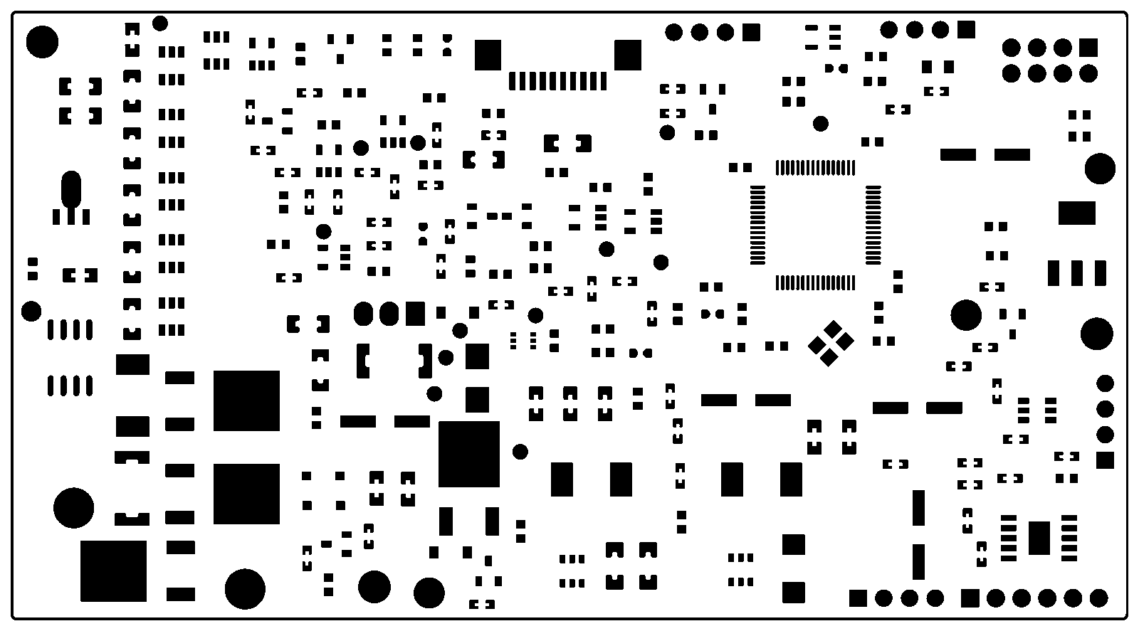
I cut my own solder paste stencils at home. Before the laser touches anything: the board outline has to go, through-hole pads take no paste so their apertures must be removed, fine-pitch apertures need shrinking or the paste bridges, and large thermal pads must be broken into a hatch grid — one big opening dumps far too much paste, and the web between apertures is what holds a home-cut stencil together.
By hand, pad by pad: an evening per board. Commercial CAM tools do it — priced for fabs, not benches.
What I built with Claude
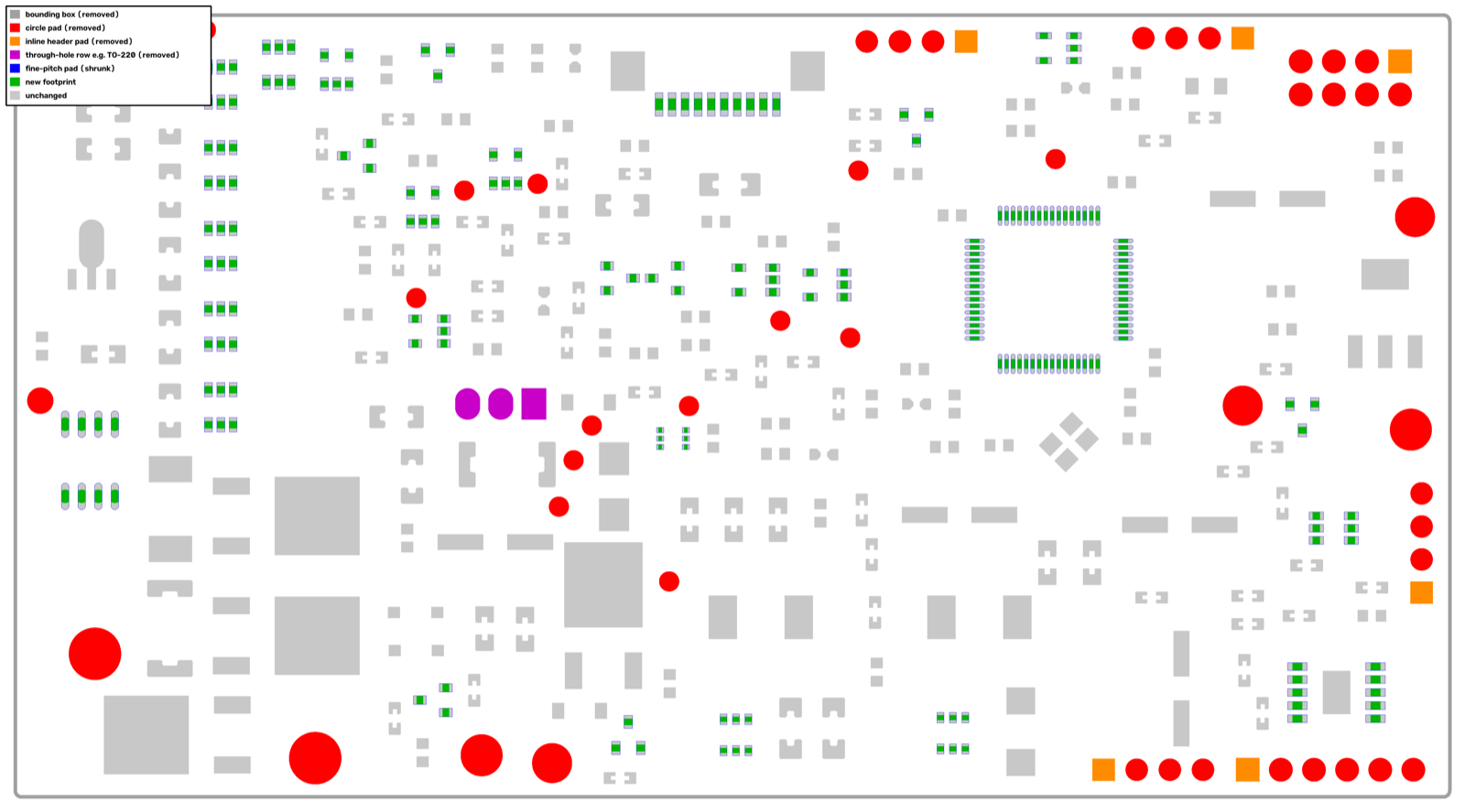
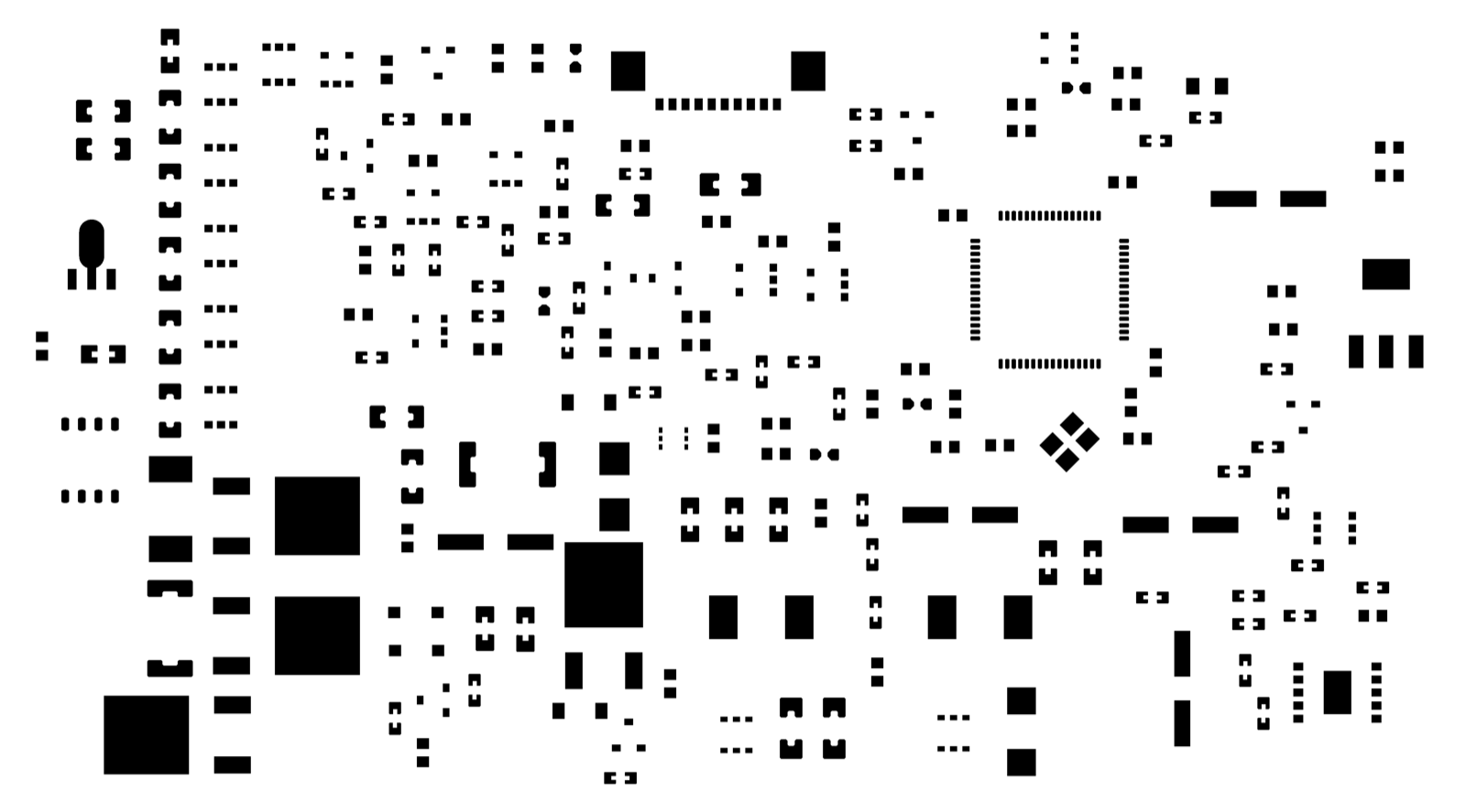
It reads the stencil PDF, derives the true scale from the page geometry, finds every aperture, classifies it, applies seven rules, and renders a colour-coded map of every decision so I can check it before committing anything to the laser.
One real board — my PowerBench.AI, 112.3 × 62.3 mm:
- 46 circular pads removed
- 3 TO-220 through-hole row pads removed
- 36 fine-pitch groups found, down to 0.50 mm pitch
- 8 SOT-23-3 transistors detected
- 211 apertures shrunk
- 4 large thermal pads converted to a 1 mm hatch grid
- 290 apertures correctly left alone
Runtime: seconds.
The part that matters
I never became an image-processing engineer. I stayed the hardware person who knows what a 0.50 mm pitch does to wet paste. Claude — Opus and Fable — brought the algorithms. I brought the boards, and the judgement about whether each answer was right.
Rule 7 gates on the pad’s short side, not its area, because a 10 × 1 mm pad has plenty of area but no room to subdivide across. Claude would not have known to make that call. I could not have implemented it. Together it took an afternoon.
I also caught two false positives by eye on the action map. Domain knowledge did not become obsolete. It became the scarce half.
The economics changed
This tool serves a market of one. No business case. Twenty years of software history says it should not exist — you adapt to whatever tool exists, or you accept the manual evening.
AI collapsed the distance between “I have a specific, annoying problem” and “there is now software that solves it.” Software shaped to my boards, my thresholds, my laser cutter — built by someone with no background in the field.
Not “AI writes apps.” Personal software: tools built for an audience of one, because building one finally costs less than living without it.
What manual task have you simply accepted, because you assumed you would need a skill you do not have?
Follow-up: I kept the transcript. 17 prompts, 53 minutes steps through the prompts that built this tool — including the thirteen words that added SOT-23 support without naming a single dimension. The tool itself is now on GitHub at MansukhPatidar/stencil.